Last updated: May 15th, 2019 at 10:08 UTC+02:00
SamMobile has affiliate and sponsored partnerships, we may earn a commission.
Reading time: 2 minutes

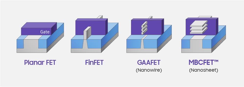
Compared to the 7nm process technology, Samsung’s 3nm gate-all-around (GAA) process, 3GAE, reduces the chip size by up to 45%, while consuming 50% less power and increasing efficiency by 35%. The process, which is a Multi-Bridge-Channel FET (MBCFET), Samsung’s patented version of GAA, uses a vertically-stacked nanosheet architecture, enabling greater current per stack compared to a FinFET process.

Samsung had already shared version 0.1 of its process design kit (PDK) with customers in April. Sharing the kit will shorten the time-to-market and improve design competitiveness for clients, the company said. Samsung has also taped out its test vehicle design and will now focus on to improve its performance and power efficiency.
Samsung also shared its process technology roadmap at the Samsung Foundry Forum. It is planning to begin the mass production of 6nm process devices in the second half of this year. The 5nm FinFET process, which was developed in April, is expected to be completed by the end of this year, with mass production scheduled for the first half of 2020. The company also expects to complete the development of its 4nm process by the end of this year. Samsung hasn't set a time frame for the 3nm GAA process yet.