MASSIVE Samsung Galaxy deals during Discover Samsung!

SamMobile has affiliate and sponsored partnerships. If you buy something through one of these links, we may earn a commission.

Samsung becomes the world’s first brand to demonstrate MRAM technology for in-memory computing

General
By 

Last updated: January 13th, 2022 at 10:06 UTC+01:00

Samsung, the world’s biggest memory chip maker, has announced that it has become the first in the world to demonstrate the MRAM (Magnetoresistive Random Access Memory) technology for in-memory computing. The company’s paper on its innovation, titled ‘A crossbar array of magnetoresistive memory devices for in-memory computing,’ was published by Nature on its website, and its print edition is coming next.

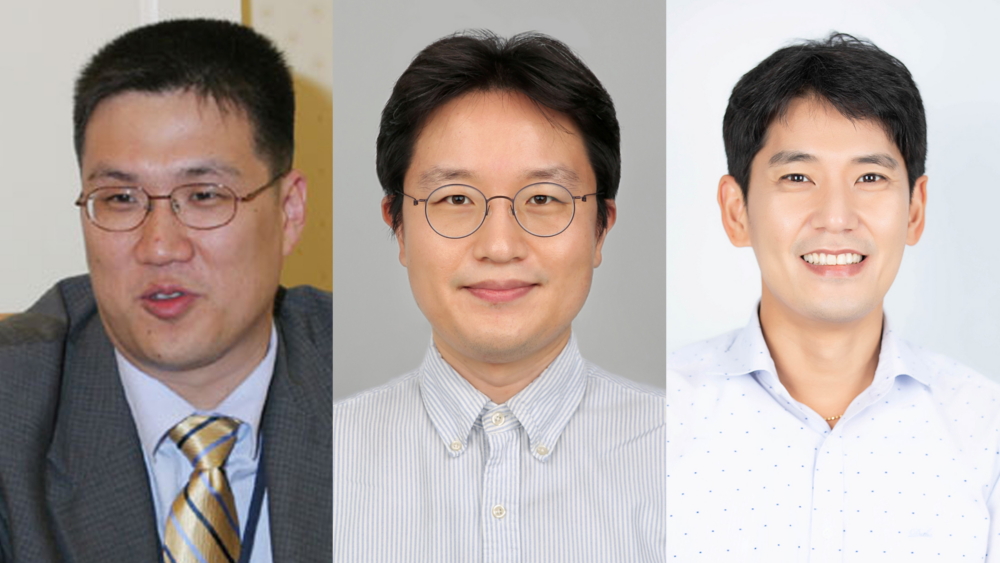
The research was a collaboration between SAIT (Samsung Advanced Institute of Technology), Samsung Foundry, and Samsung Semiconductor R&D. Dr. Seungchul Jung (Staff Researcher at SAIT), Dr. Donhee Ham (Fellow of SAIT and Professor of Harvard University), and Dr. Sang Joon Kim (Vice President of Technology at SAIT) worked on the research.

Usually, data is stored in memory chips (DRAM) and processed by a CPU or an AP (Application Processor). However, data storage and computing happen on the same chip with in-memory computing. Since there is no need to transfer data from memory to the processor and vice versa, a lot of time is saved. Data processing inside the memory happens in a highly parallel manner, resulting in substantial power savings. Samsung claims that MRAM technology will be great for things like AI processing.

Other in-memory computing solutions like PRAM (Phase-change Random Access Memory) and RRAM (Resistive Random Access Memory) have been demonstrated worldwide, but MRAM has been difficult to prove. Despite MRAM’s non-volatile nature, high operational speed, and endurance, it was difficult to use it for in-memory computing due to its low resistance. It was also impossible to use MRAM’s power efficiency advantage in a standard in-memory computing architecture.

Samsung has now created a solution to the problem through its new architecture innovation. The South Korean firm developed an MRAM array chip that uses ‘Resistance Sum’ instead of the standard ‘Current-Sum.’ The new solution counters the problem of small resistances of individual MRAM devices.

The company’s new MRAM in-computing was tested by running AI applications, and it offered 98% accuracy in the classification of handwritten digits and 93% accuracy in detecting faces in images. Samsung says that its new technology can be used to make highly power-efficient AI chips.

Dr. Seungchul Jung, the first author of the paper, said, “In-memory computing draws similarity to the brain in the sense that in the brain, computing also occurs within the network of biological memories, or synapses, the points where neurons touch one another. In fact, while the computing performed by our MRAM network for now has a different purpose from the computing performed by the brain, such solid-state memory network may in the future be used as a platform to mimic the brain by modeling the brain’s synapse connectivity.

Join SamMobile’s Telegram group and subscribe to our YouTube channel to get instant news updates and in-depth reviews of Samsung devices. You can also subscribe to get updates from us on Google News and follow us on Twitter.

General MRAMSamsung FoundrySamsung Semiconductor
Load comments

You might also like

Japan’s government wants to help Samsung build its chip factory

Japan’s government wants to help Samsung build its chip factory

Samsung could be planning on building a new semiconductor manufacturing facility in Japan. The facility would include Samsung’s first chip packaging test line in the country, and a new report says that the Japanese government is willing to offer subsidies worth roughly 15 billion yen ($110 million) to the Korean tech giant, should the latter […]

  • By Mihai Matei
  • 8 hours ago
As Apple hoards TSMC’s 90% 3nm chip capacity, others could turn to Samsung for chips

As Apple hoards TSMC’s 90% 3nm chip capacity, others could turn to Samsung for chips

Samsung Foundry and TSMC are the only companies in the world capable of making chips using advanced fabrication processes. While Samsung Foundry started the production of semiconductor chips using its first-generation 3nm GAA process in the second half of 2022, TSMC has just begun making 3nm chips for Apple. Since Apple has booked almost all […]

  • By Asif Iqbal Shaik
  • 1 day ago
Samsung may be developing Shinebolt and Flamebolt DRAM for AI supercomputers

Samsung may be developing Shinebolt and Flamebolt DRAM for AI supercomputers

A couple of weeks ago, a mysterious trademark application revealed that Samsung is trying to secure the term “Snowbolt” for an unreleased product that has everything to do with DRAM (Dynamic Random Access Memory). In the meantime, two more trademark applications related to DRAM have emerged, confirming that whatever Snowbolt is, it won’t be alone. […]

  • By Mihai Matei
  • 2 days ago
Tesla CEO Elon Musk meets Samsung boss Lee Jae-yong to discuss car chips

Tesla CEO Elon Musk meets Samsung boss Lee Jae-yong to discuss car chips

Tesla CEO Elon Musk met Samsung Electronics Executive Chairman Lee Jae-yong for the first time during the latter’s recent business trip to the US. The two top-level executives discussed ways to collaborate on automotive semiconductor chips. The meeting was held at Samsung Research America Headquarters in Silicon Valley, California, USA. Reports suggest that Elon Musk […]

  • By Asif Iqbal Shaik
  • 3 days ago
Samsung is building a $222 million chip development facility in Japan

Samsung is building a $222 million chip development facility in Japan

Samsung, the world’s biggest memory chip maker, is reportedly building a new chip development facility in Yokohama, Japan. This highly symbolic initiative will bring together Japanese and South Korean chip firms to combat competition from the Chinese and Taiwanese markets. This new chip development facility will cost over JPY 300 billion (around $222 million) and […]

  • By Asif Iqbal Shaik
  • 3 days ago
Oppo shuts down own chip division and potential Samsung Foundry client

Oppo shuts down own chip division and potential Samsung Foundry client

Oppo can no longer support the Chinese government’s dream of becoming self-sufficient in the semiconductor sector. New reports say that the company has suddenly shut down its chip design business to the shock of its employees. News about the smartphone maker establishing an in-house chip design team emerged in December 2022. Back then, rumors said […]

  • By Mihai Matei
  • 5 days ago