Last updated: June 22nd, 2020 at 20:02 UTC+02:00
SamMobile has affiliate and sponsored partnerships, we may earn a commission.
Reading time: 2 minutes
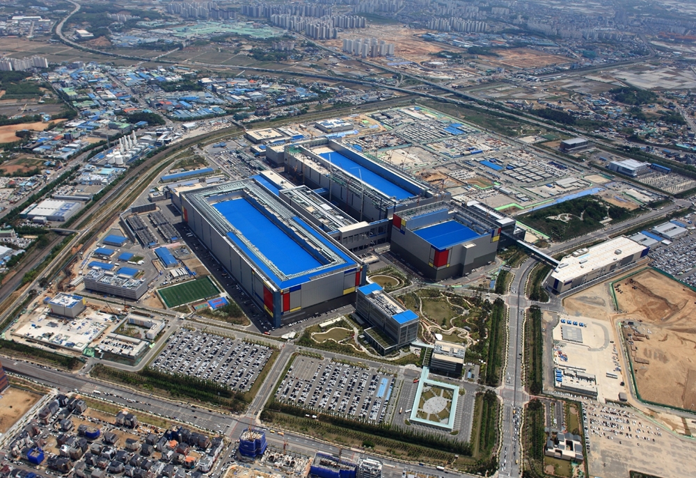
The P3 plant will reportedly be 300 meters longer than the existing P2 plant, topping a total of 700 meters in length. Constructing the building itself should take roughly a year, and a few additional months will be needed to install the necessary equipment and ready it for mass production.
Given the size of the P3 plant compared to the P2 factory, industry watchers speculate that Samsung might want to turn the P3 facility into a ‘total semiconductor factory' capable of producing DRAM and NAND flash chips as well as system semiconductors including application processors and image sensors. The P3 plant will also reportedly be the place where future manufacturing processes will debut before they'll be adopted by Samsung's other manufacturing facilities.
Samsung is the largest DRAM and NAND flash manufacturer in the world and it dominated the smartphone memory market all throughout 2019. It manufactures semiconductor solutions for its own products as well as for numerous major clients. Demand for newer memory technologies is likely to increase and the company wants to keep the momentum going. If the reports turn out to be accurate, its giant P3 plant in Pyeongtaek could be a key component for the company to maintain its leading role in the segment.

First Samsung device: SGH-A800
Mihai is a blogger and column writer at SamMobile. His first Samsung phone was an A800 which took a lot of beating, and a part of him still misses the novelty of the clamshell design. In his free time, he enjoys watching shows, documentaries, and stand-up comedy; listening to music, taking walks, and occasionally playing old(er) video games.