Last updated: February 4th, 2020 at 07:19 UTC+01:00
SamMobile has affiliate and sponsored partnerships, we may earn a commission.
Reading time: 2 minutes
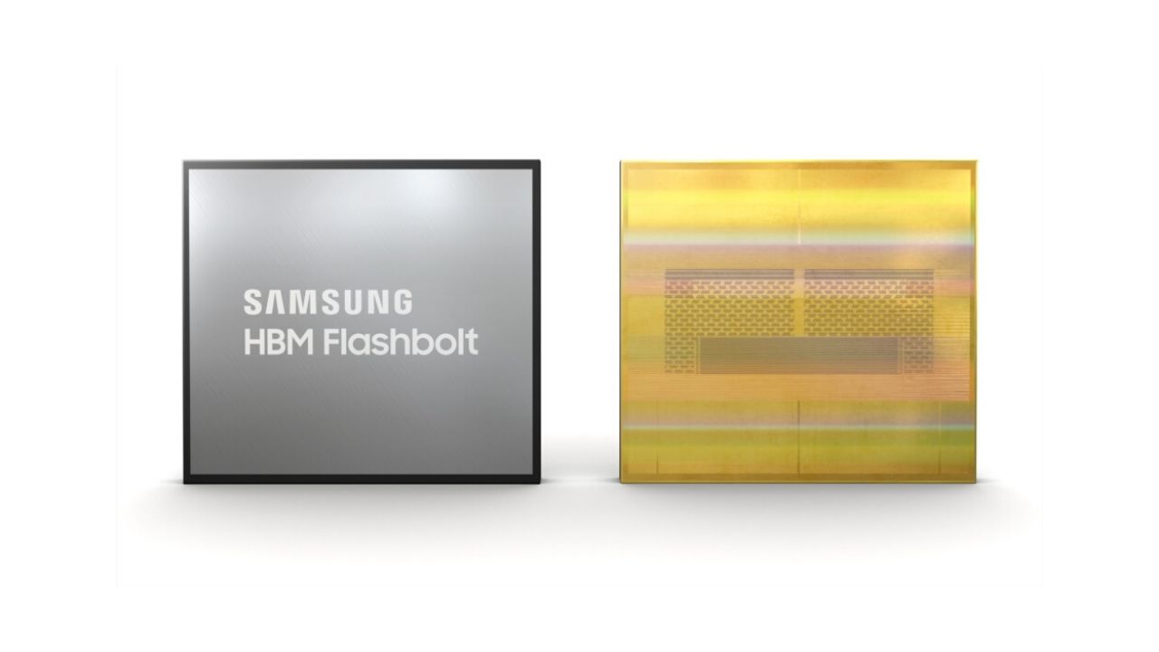
One year after releasing the HBM2 ‘Aquabolt' memory, the South Korean chip giant had initially announced the Flashbolt HBM memory last year during Nvidia's 2019 GTC (GPU Technology Conference). This memory technology will likely be used in upcoming high-end GPUs from AMD and Nvidia. Late last month, JEDEC (Joint Electron Tube Engineering Council) had published an updated revision of the HBM2 standard.
Samsung's HBM2E memory can reach maximum data transfer speeds of up to 3.2Gbps per pin. Up to eight 8Gb DRAM chips can be vertically stacked on top of a buffer chip to achieve 16GB package capacity. The company is manufacturing these chips using its 10nm (1y) fabrication technology. The memory bandwidth per stack is 410GB/s.
When overclocked, these HBM2E memory chips can offer up to 4.2Gb/s data transfer rates per pin and a memory bandwidth of 538GB/s. In comparison, the second-generation HBM memory from the company offered 2.4Gb/s bandwidth per pin, 307.2GB/s bandwidth per stack, and 8GB total capacity.
Samsung says that these DRAM chips will go into mass production in the first half this year. The South Korean firm will continue to offer HBM2 Aquabolt memory to its ecosystem partners.

First Samsung device: T100
Asif is a computer engineer turned technology journalist. He has been using Samsung phones since 2004, and his current smartphone is the Galaxy S23 Ultra. He loves headphones, mechanical keyboards, and PC hardware. When not writing about technology, he likes watching crime and science fiction movies and TV shows.