Last updated: August 13th, 2020 at 06:27 UTC+02:00
SamMobile has affiliate and sponsored partnerships, we may earn a commission.
Reading time: 2 minutes
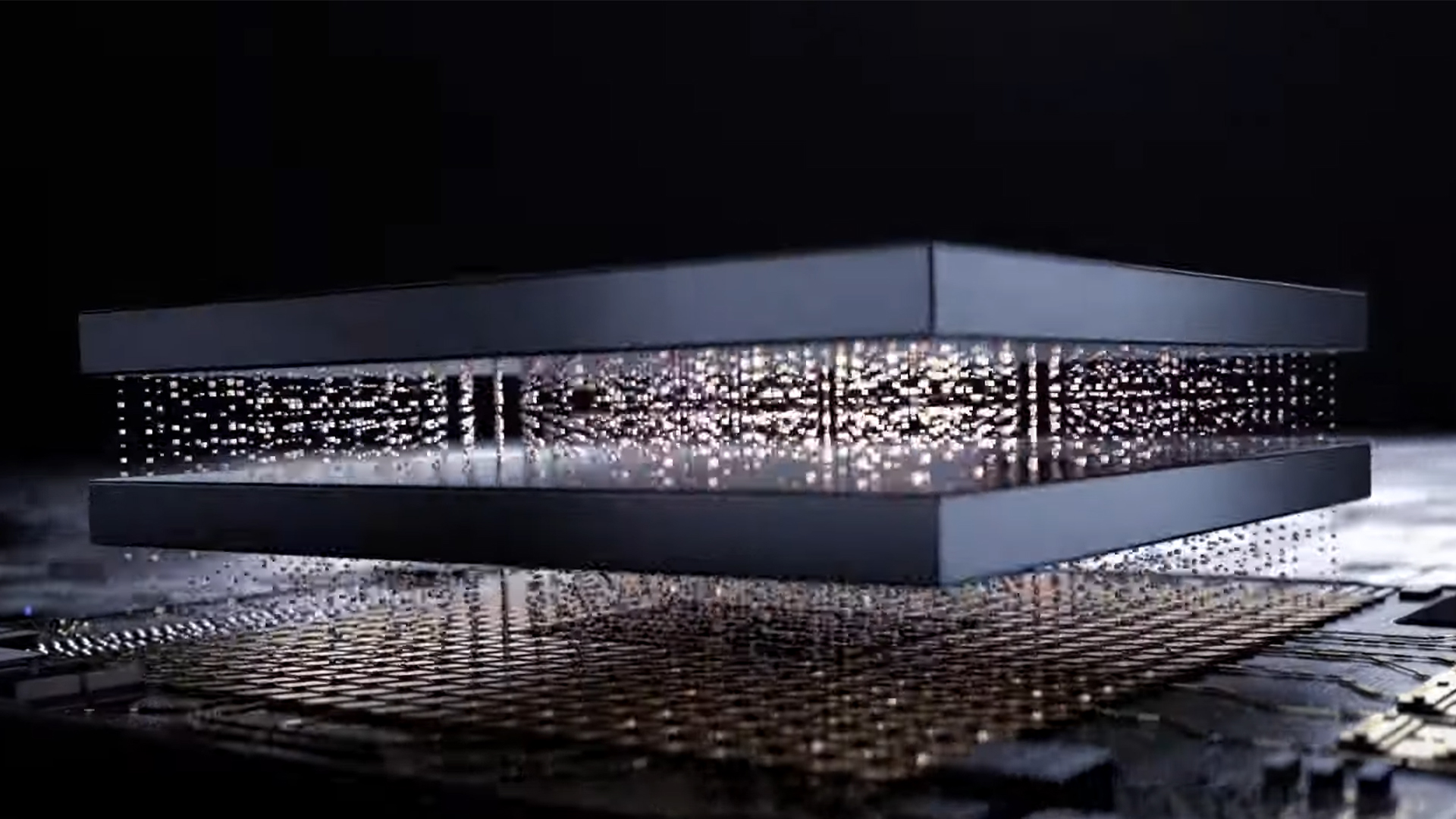
The company's contract chip manufacturing arm, Samsung Foundry, has completed the production of test chips using the X-Cube (or Extended Cube) technology. The new 3D integrated circuit chip packaging technology is now available to manufacture 7nm chips. It allows ultra-thin stacking of multiple chips to make a more compact logic semiconductor. The process uses through-silicon via (TSV) technology for vertical electrical connection instead of using wires.
Samsung claims that chip designers can use its X-Cube technology to design custom chips that are best suited to their unique needs. Thanks to the TSV technology, the signal paths between different stacks in a chip are significantly reduced, increasing the data transfer speeds and energy efficiency. Various logic blocks, memory, and storage chips can be stacked on top of one another to create more compact silicon packages.
The company says that this technology will be used in 5G, AI (artificial intelligence), AR (augmented reality), HPC (high-performance computing), mobile, and VR (virtual reality) segments. Samsung Foundry will showcase its new technology during the Hot Chips 2020 expo, which runs from August 18 to August 20. It is also working on improving the 5nm process and skipping 4nm to develop 3nm technology for the near future.

First Samsung device: T100
Asif is a computer engineer turned technology journalist. He has been using Samsung phones since 2004, and his current smartphone is the Galaxy S23 Ultra. He loves headphones, mechanical keyboards, and PC hardware. When not writing about technology, he likes watching crime and science fiction movies and TV shows.