Last updated: March 19th, 2024 at 17:28 UTC+01:00
SamMobile has affiliate and sponsored partnerships, we may earn a commission.
Reading time: 2 minutes
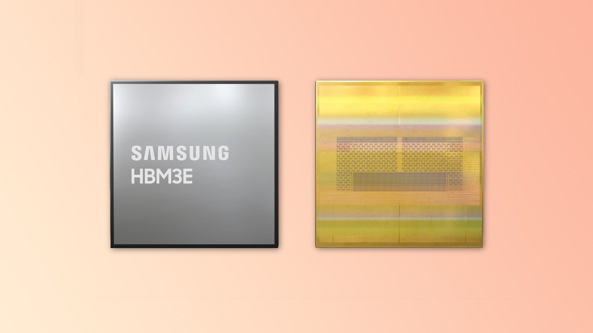
SK Hynix has managed to establish a solid footing for itself in the HBM market. Samsung, a longstanding dominant force in the memory market, would certainly want as much share for itself as it can possibly grab. However, the company has denied that it's going to use the same tech that SK Hynix does.
Samsung's HBM chips are made using the non-conductive film method that stacks layers of chips. This method is said to work well for chips with fewer layers but it presents issues in chips with a greater number of layers, thus resulting in lower yields. That's said to be one of the reasons why Samsung is behind in the HBM space to supply leading AI chip manufacturers like NVIDIA with HBM3 chips.
SK Hynix utilizes the mass reflow molded underfill process which apparently doesn't suffer from the same shortcomings and provides a yield of 60-70%. That's what has enabled SK Hynix to gain a commanding position in the market and also ink a recent deal with NVIDIA to supply HBM3 chips.
However, Samsung would like everyone to know that there's no truth to these reports. In a short statement, a spokesperson for the company confirmed that “Rumors that Samsung Electronics will apply MR-MUF to its HBM production are not true.” The spokesperson also dismissed reports about low yields, saying that Samsung has continued to maintain a stable yield rate of its HBM3 chips.

Adnan Farooqui is a long-term writer at SamMobile. Based in Pakistan, his interests include technology, finance, Swiss watches and Formula 1. His tendency to write long posts betrays his inclination to being a man of few words.


