


Latest opinions
-
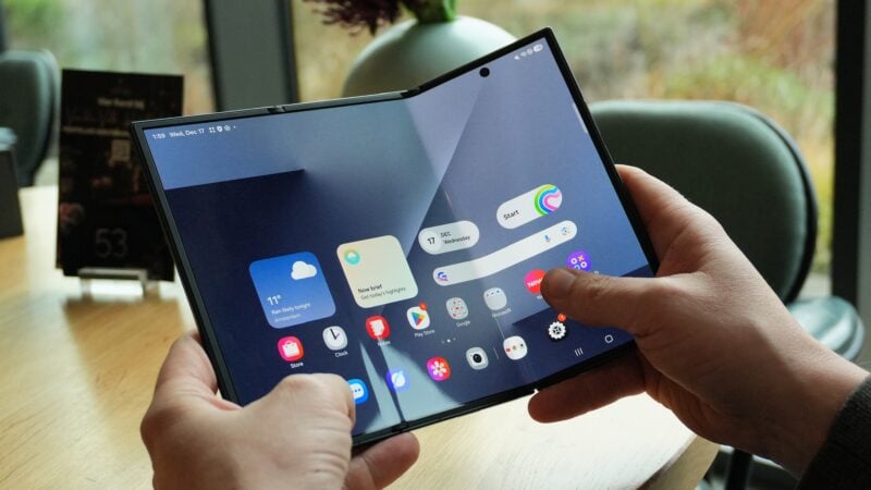
 Apple has no answer to the Galaxy Z Fold 8 Ultra, and Samsung should pounce on it
 -
 Meta just showed Samsung what Galaxy Glasses don't need to become
 -
 Mirror view missing from the Galaxy Z Fold 8 feels like another weird Samsung omission
 -
 iPhone Duo hype proves Samsung was right about foldables all along
 -
 I'm going on holiday, and my Galaxy Z Fold 8 isn't coming with me
 -
 Apple's Siri AI troubles prove Samsung's messy multi-AI strategy was right
 -
 Apple just showed Samsung what foldable buyers care about
 -
 7 years of foldables and my Galaxy Z Fold 8 still can't count screen usage properly
 -
 The Galaxy Z Fold 8 may hold the answer to the only viable compact phone formula



