SamMobile has affiliate and sponsored partnerships. If you buy something through one of these links, we may earn a commission.

Notifications
    News for you

    Samsung develops industry’s first 36GB HBM3E 12H DRAM

    General
    By 

    Last updated: February 26th, 2024 at 20:01 UTC+01:00

    Samsung, the world leader in semiconductor memory chips, has announced that it has developed the industry's first 12-stack HBM3E DRAM chip. It is the world's highest-capacity HBM memory chip to date, and the company claims that it offers 50% higher capacity and performance than previous-generation HBM memory chips.

    Samsung unveils industry's first 36GB HBM3E DRAM chip

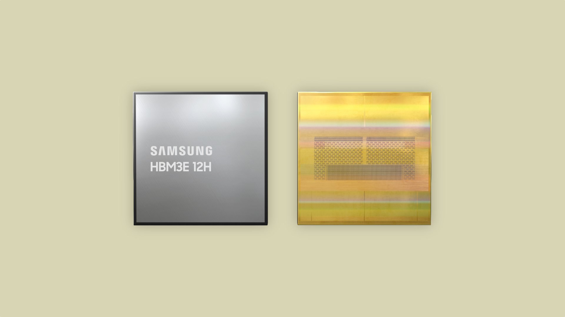
    According to Samsung, its HBM3E 12H chip offers a bandwidth of up to 1,280GB/s and a capacity of up to 36GB. That is 50% higher than current-generation HBM3 8H chips with eight stacks.

    It uses an advanced Thermal Compression Non-Conductive Film (TC NCF) that allows 12-layer products to have the same height as 8-layer HBM chips. This eases compatibility and improves the flexibility of system builders. It also offers added benefits, including mitigating chip die wrapping that comes with a thinner die.

    Samsung says that its HBM3E chips have the industry's smallest gap between chips: 7µm. This eliminates voids between the layers inside the chip and enhances vertical density by 20% compared to 8-layer HBM3 chips.

    Samsung HBM3E 12H DRAM

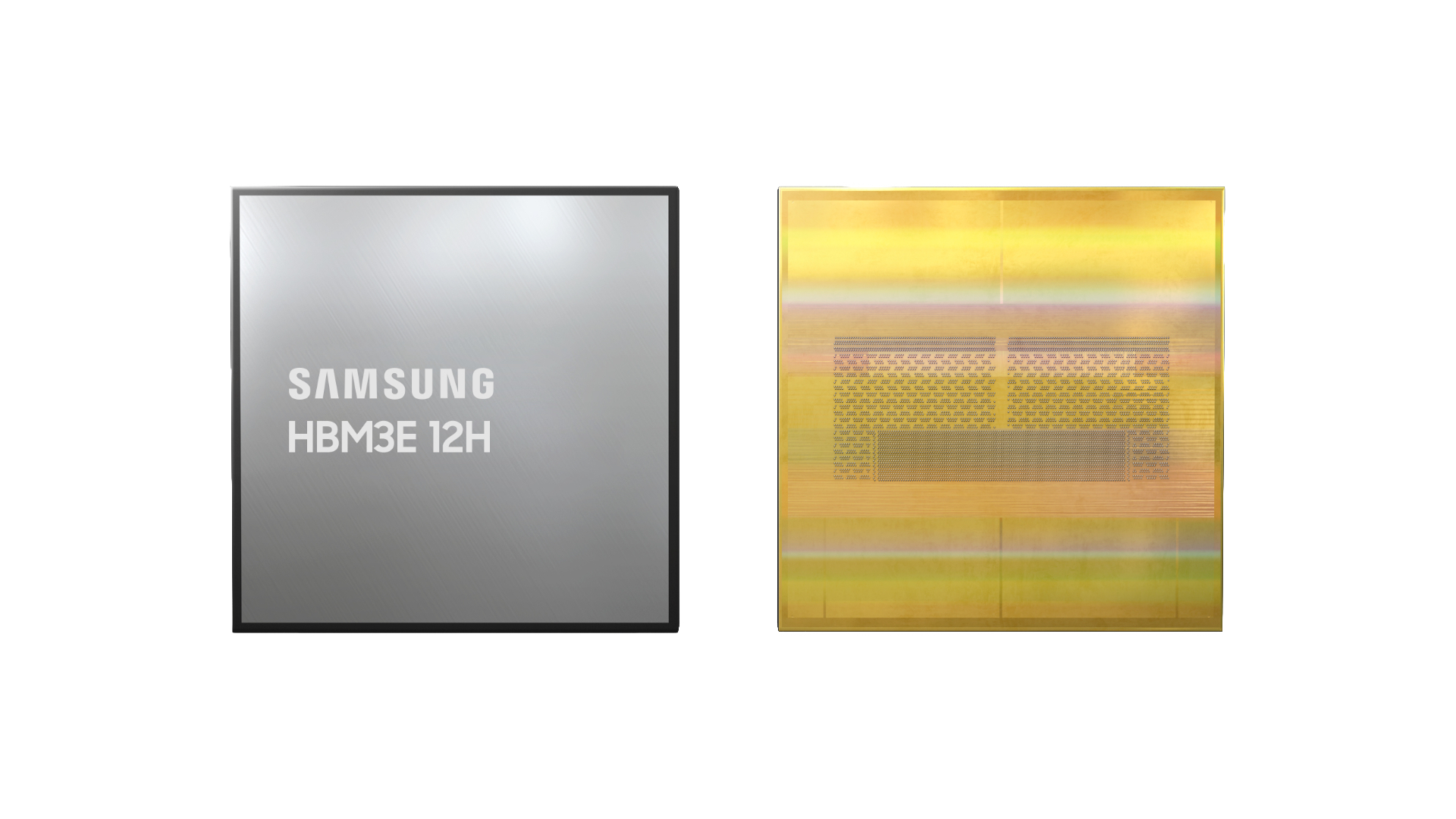
    Samsung's new TC NCF technology improves thermals inside HBM chips by using bumps of varying sizes between the chips. Smaller bumps are used in areas for signaling, while larger bumps are used in spots that require heat dissipation. Samsung claims that this method also improves the yield of the product. These chips can be used in systems that require higher memory capacity.

    HBM3E chips can increase AI training speed by 34%

    Enterprises using these new chips can get higher performance and capacity and reduce the total cost of ownership in data centers. When used for AI applications, the average speed of AI training can be completed 34% faster, while simultaneous uses of services can be increased by 11.5 times.

    Samsung says it has begun sending samples of its HBM3E 12H chips to customers, and mass production will begin in the first half of this year.

    Yongcheol Bae, Executive Vice President of Memory Product Planning at Samsung Electronics, said, “The industry's AI service providers are increasingly requiring HBM with higher capacity, and our new HBM3E 12H product has been designed to answer that need. This new memory solution forms part of our drive toward developing core technologies for high-stack HBM and providing technological leadership for the high-capacity HBM market in the AI era.

    General DRAMHBMHBM3ESamsung Semiconductor Buy Galaxy Watch 6

    You might also like

    Samsung profit jumps 933% to $4.8 billion in Q1 2024, beating estimates

    Samsung profit jumps 933% to $4.8 billion in Q1 2024, beating estimates

    Samsung has revealed its financial results for the first quarter of this year, a few weeks after revealing revenue estimates. The company revealed that its revenue rose 13% compared to Q1 2023, while its profit skyrocketed nearly 10x (933%) compared to the year earlier. Samsung's profit jumps nearly 10x in Q1 2024, thanks to strong […]

    • By Asif Iqbal Shaik
    • 7 days ago
    AMD will pay Samsung $3 billion for a crucial part used in AI chips

    AMD will pay Samsung $3 billion for a crucial part used in AI chips

    Companies making AI semiconductors need a lot of high-bandwidth memory chips, and Samsung has advanced memory chips to sell. The company has been winning major orders from leading companies as it seeks to establish a dominant position in the HBM3E segment, where local rival SK Hynix has gained a considerable market share. A news report […]

    • By Adnan Farooqui
    • 2 weeks ago
    Samsung is world’s first to start mass production of 1Tb 9th Gen. V-NAND chips

    Samsung is world’s first to start mass production of 1Tb 9th Gen. V-NAND chips

    Samsung, the world's biggest memory chip maker, has announced it is the first brand to start mass-producing 1Tb TLC 9th Gen V-NAND flash chips. TLC refers to Triple Level Cell, and the new chips can store 3-bit data in one cell. Samsung becomes world's first brand to start mass production of 1Tb 9th Generation V-NAND […]

    • By Asif Iqbal Shaik
    • 2 weeks ago
    Galaxy S25’s Exynos 2500 to be more efficient than Snapdragon 8 Gen 4

    Galaxy S25’s Exynos 2500 to be more efficient than Snapdragon 8 Gen 4

    Samsung is developing the Exynos 2500 chipset, which it could offer with the Galaxy S25 series smartphones in some regions. Last year, the company confirmed that it would make the upcoming chipset on Samsung Foundry’s second-generation 3nm fabrication process, which is expected to offer better power efficiency than not only Samsung’s 4nm fabrication process that […]

    • By Abid Iqbal Shaik
    • 3 weeks ago
    Samsung has a grand plan to establish dominance in AI memory

    Samsung has a grand plan to establish dominance in AI memory

    The demand for high-bandwidth memory (HBM) is projected to skyrocket in the coming years as AI matures and the era of general artificial intelligence is ushered in. As one of the world's leading suppliers of memory products, Samsung understandably considers this a lucrative opportunity, and the company has put together a grand plan to establish […]

    • By Adnan Farooqui
    • 3 weeks ago
    Samsung unveils world’s first 10.7Gbps LPDDR5X DRAM chip, designed for AI

    Samsung unveils world’s first 10.7Gbps LPDDR5X DRAM chip, designed for AI

    Samsung, the world's biggest memory chip manufacturer, has unveiled its fastest LPDDR5X DRAM chip. The new chip can attain data transfer speeds of up to 10.7Gbps, higher than the 6.4Gbps LPDDR5X chip launched in 2021 and the 8.5Gbps LPDDR5X DRAM chip unveiled in 2022. Samsung's new LPDDR5X DRAM chips will be available in late 2024 […]

    • By Asif Iqbal Shaik
    • 3 weeks ago