

Latest opinions
-
 Expectations vs reality: What does the Galaxy Z Fold 8's foldable screen actually feel like?
 -
 Is Samsung building the Galaxy S27 Pro with everyone else’s features?
 -
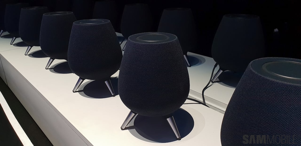 A critical piece is missing from Samsung's smart home ecosystem
 -
 Samsung could crush Apple with the Galaxy Z Fold 8 and Fold 9
 -
 iPhone Duo pre-orders show Apple users are watching Samsung’s innovations closely
 -
 Samsung has a reason to make fewer Galaxy phones, and it's a risk worth taking
 -
 Even a 1TB Galaxy Z Fold 8 can cost less than a 256GB iPhone Duo
 -
 I can't stand this One UI feature many Galaxy Z Fold users seem to love
 -
 Why Samsung needs to double down on the bet it has made on 82 million US Galaxy devices