We got the best Samsung deals! Galaxy S24 Ultra, Watch 6, Z Fold 5 or, Z Flip 5.

SamMobile has affiliate and sponsored partnerships. If you buy something through one of these links, we may earn a commission.

Notifications
    News for you

    Samsung semiconductor plants receive important environment certification from UL

    General
    By 

    Last updated: June 11th, 2020 at 08:38 UTC+02:00

    Samsung is the biggest memory chip manufacturer, and it is counted among the largest semiconductor manufacturers in the world. Now, all semiconductor manufacturing facilities of the company have received the Zero Waste to Landfill certification with the Gold classification or above from UL (Underwriters Laboratories). This validation shows that the company's facilities are environmentally friendly.

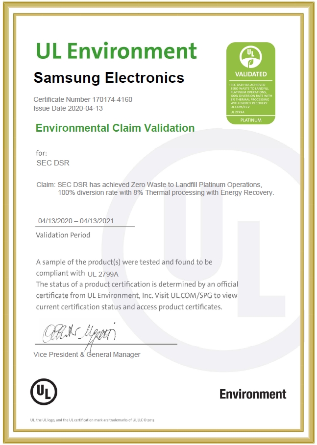
    The company's global semiconductor manufacturing sites in China, South Korea, and the US meet the requirement of more than 95-percent waste diversion through methods that do not involve thermal processing. The Samsung DSR building in Hwaseong, Korea, has received the Platinum classification with 100-percent waste diversion. This is where most of the company's local semiconductor R&D staff live.

    The South Korean chip giant's semiconductor plant in Austin, Texas, in the US, was the first one to receive UL's Zero Waste to Landfill certification. It won the validation in January. Later, five facilities in South Korea (Cheonan, Giheung, Hwaseong, Onyang, and Pyeongtaek) and two facilities in China (Suzhou and Xi'an) were granted environmental certifications.

    Underwriters Laboratories is a third-party industry testing and certification organization. It designed the Zero Waste to Landfill validation program to minimize the environmental footprint of industries by shifting waste management methods from thermal processing or landfill disposal to safer methods like recycling and reusing. It also includes employee awareness and waste reduction campaigns.

    Chanhoon Park, Executive Vice President of Global Infrastructure Technology, Samsung Electronics, said, “The Zero Waste to Landfill Gold validation is a testament to the care and effort by our employees around the world to protect the environment. Eco-friendly operations are now a must for any business, and we will continue to ensure sustainable growth that is mindful of the environment that we live and operate in.

    Samsung's semiconductor manufacturing facilities getting reviewed and certified by UL is an achievement. The milestone shows the company's commitment to the environment and the health of its 60,000 employees across its eight chip production sites. UL has also certified Samsung's batteries, smartphones, smartphone displays, and TVs for greater efficiency, environmental friendliness, and safety in the past.

    Samsung Semiconductor Zero Waste To Landfill - Waste Management Certification Underwriters Laboratories

    General Samsung Semiconductor

    You might also like

    Next-gen Galaxy phones will have faster storage for on-device AI

    Next-gen Galaxy phones will have faster storage for on-device AI

    It's been a couple of years since Samsung Semiconductor announced the UFS 4.0 non-volatile memory for mobile devices. Samsung has since used UFS 4.0 for the Galaxy S23 series, the 2023 foldable phones, and the latest Galaxy S24 lineup. Now, the company is getting ready to advance to the next step. Samsung Semiconductor revealed a […]

    • By Mihai Matei
    • 5 days ago
    Samsung to launch its own AI accelerator chip called Mach-1 in 2025

    Samsung to launch its own AI accelerator chip called Mach-1 in 2025

    Samsung launched its first AI phone, the Galaxy S24, earlier this year. Before that, the South Korean firm launched its own Large Language Model (LLM) called Samsung Gauss, which powers some of the AI features on the Galaxy S24. It is reported that Samsung will launch its own AI accelerator chip next year. Samsung's first […]

    • By Asif Iqbal Shaik
    • 6 days ago
    Samsung expects $100 million revenue from chip packaging business

    Samsung expects $100 million revenue from chip packaging business

    Samsung Electronics held its 55th annual general shareholders meeting today at the Suwon Convention Center in Suwon, Gyeonggi-do, South Korea. The company revealed its strategy for this year and expects revenue of $100 from its chip packaging business. The company's 55th annual general shareholders meeting was attended by general shareholders, institutional investors, and top-level management […]

    • By Asif Iqbal Shaik
    • 6 days ago
    Samsung could get $6 billion grant from the US for chip plants

    Samsung could get $6 billion grant from the US for chip plants

    Samsung Electronics, one of the biggest chip-making firms worldwide, has grand plans to make advanced semiconductor chips in the US. To help with its plans, the US government had announced grants and tax sops. The South Korean firm is now close to getting a huge helping hand from the US government. A $6 billion grant […]

    • By Asif Iqbal Shaik
    • 2 weeks ago
    Samsung may use SK Hynix’s method to manufacture HBM3 chips

    Samsung may use SK Hynix’s method to manufacture HBM3 chips

    According to a new report from Reuters, Samsung Electronics will soon start using the same technology as SK Hynix does to manufacture HBM3 chips. Samsung uses the non-conductive film (NCF) method to stack layers of chips in high bandwidth memory (HBM) chips. Reportedly, this method works well for chips with a lower number of layers […]

    • By Abid Iqbal Shaik
    • 2 weeks ago
    Samsung has a plan to reap more profits this year

    Samsung has a plan to reap more profits this year

    2023 was a bad year for Samsung, as the demand for chips fell along with their prices. The company's cash cow reported a loss for the first time in its history. As a result, Samsung Electronics' profit was the lowest in recent years. However, things are expected to improve in the coming months, and Samsung […]

    • By Asif Iqbal Shaik
    • 2 weeks ago