Last updated: December 21st, 2023 at 14:38 UTC+01:00
SamMobile has affiliate and sponsored partnerships, we may earn a commission.
Reading time: 2 minutes
It is being reported that Samsung is investing in a new chip research facility to develop advanced chip packaging technologies. The company was looking to set up a chip packaging facility in Kanagawa prefecture to deepen its business ties with Japanese firms that make chip equipment and materials. Samsung already has a research and development center in the area. Japan's industry ministry has announced that it will offer subsidies of up to JPY 20 billion ($140 million) to resurrect the local chip development and manufacturing ecosystem.
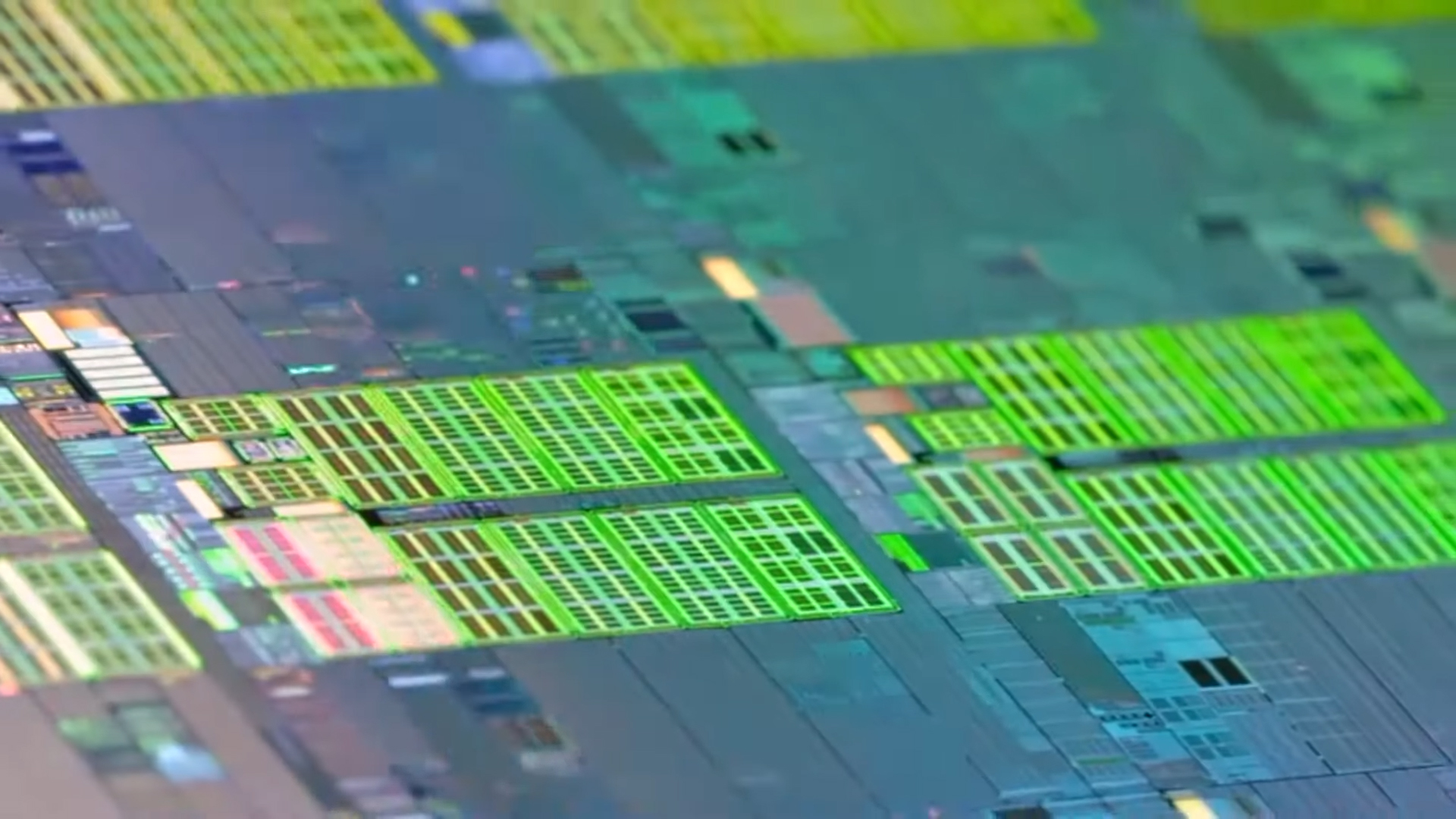
The South Korean chip giant is investing in Japan at a crucial time when tensions are arising between China and the alliance of Japan and the US. Samsung started improving its chip packaging technologies last year to gain technological superiority over others. Chip packaging involves packing several components on a single chip for a more compact chip and improved power efficiency.
Right now, Samsung is the second-biggest semiconductor chip maker in the world, but its foundry market share is way lower than its Taiwanese rival, TSMC. The company is planning to invest $230 billion over the next few years to overthrow TSMC and become the world's biggest chip maker.

Asif is a computer engineer turned technology journalist. He has been using Samsung phones since 2004, and his current smartphone is the Galaxy S23 Ultra. He loves headphones, mechanical keyboards, and PC hardware. When not writing about technology, he likes watching crime and science fiction movies and TV shows.