Must have deals! Today: Galaxy S23 Ultra and the Galaxy Buds 2 Pro!

SamMobile has affiliate and sponsored partnerships. If you buy something through one of these links, we may earn a commission.

Samsung’s 2.5D chip packing technology H-Cube is now available

General
By 

Last updated: November 11th, 2021 at 07:46 UTC+01:00

Samsung Foundry has announced that its latest 2.5D semiconductor chip packaging technology H-Cube is now available for its foundry clients. H-Cube, which was developed in collaboration with Samsung Electro-Mechanics and Amkor Techology, allows complex logic and HBM (High-Bandwidth Memory) chips to be packed in compact sizes.

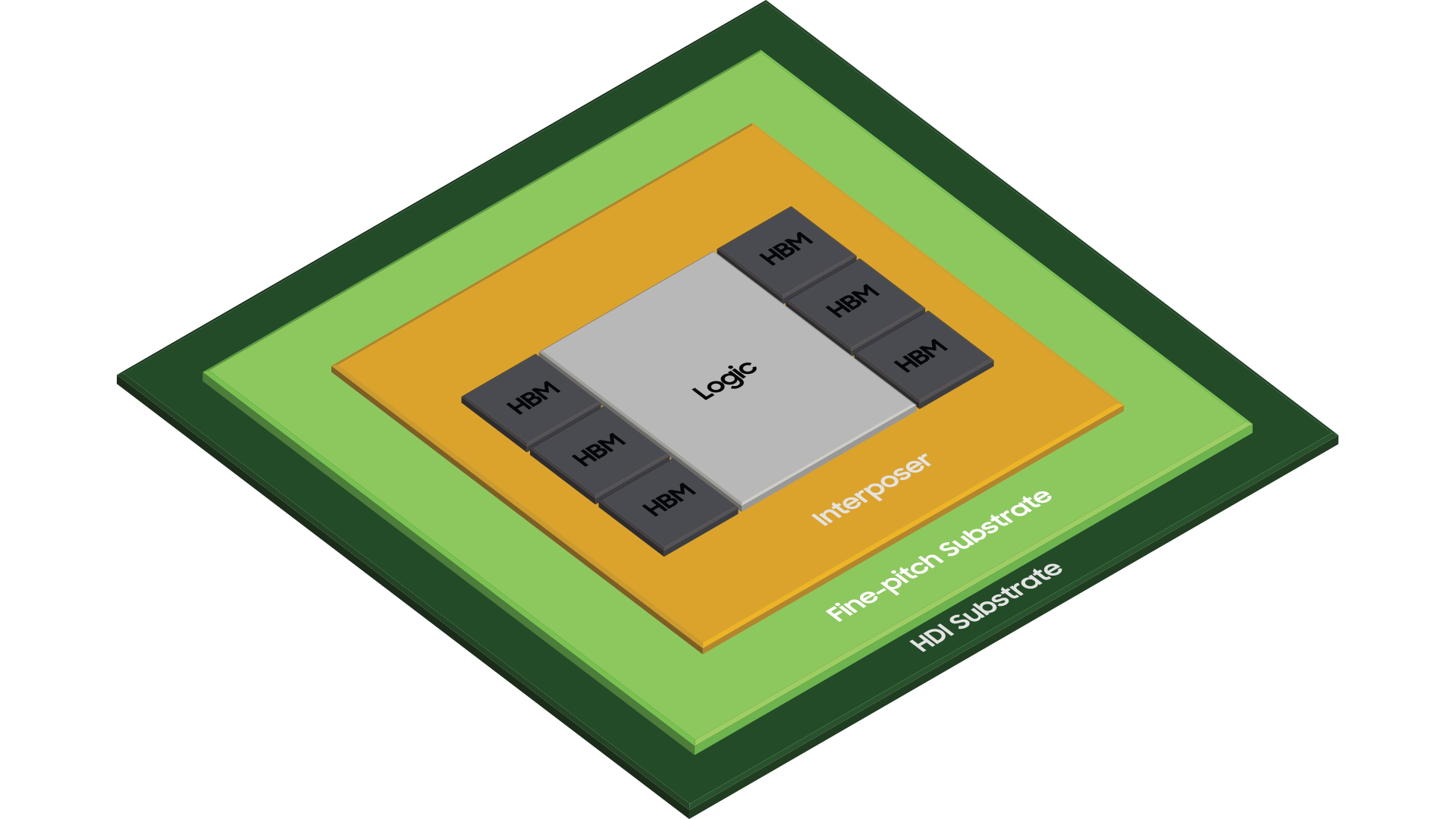
The South Korean firm said that its new packaging technology is suitable for AI (Artificial Intelligence), data center, HPC (High-Performance Computing), and networking products that require high-performance and large-area packaging. This technology can be used to place logic chips or HBM on top of a silicon interposer in a smaller area.

To develop this technology, Samsung Foundry used a hybrid substrate with a fine-pitch substrate and High-Density Interconnection (HDI) to fit large sizes into 2.5D packaging. With increasing computing power and storage needs, semiconductor chips can become larger in size, but 2.5D chip packaging technology like H-Cube can fit more in a smaller area and offer compact solutions.

When fitting six or more HBMs in a single package, difficulty in making the package can increase rapidly. Samsung solved this issue by using a hybrid substrate structure that uses an easy-to-implement HDI substrate overlapped under a fine-pitch substrate. The company also used solder balls with a smaller pitch (35%) to connect the chip with the substrate.

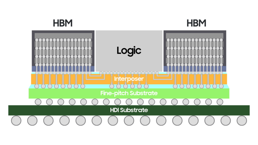
The company also used its proprietary signal/power integrity analysis technology for a stable power supply and less distortion when stacking logic chips on top of HBM.

said Moonsoo Kang, Senior Vice President and Head of Foundry Market Strategy Team at Samsung Electronics, said, “H-Cube solution, which is jointly developed with Samsung Electro-Mechanics (SEMCO) and Amkor Technology, is suited to high-performance semiconductors that need to integrate a large number of silicon dies. By expanding and enriching the foundry ecosystem, we will provide various package solutions to find a breakthrough in the challenges our customers are facing.

Samsung H-Cube 2.5 Chip Packaging Technology Structure Top View

General HBMSamsung Electro-MechanicsSamsung Foundry

You might also like

More info about Pixel 9’s Tensor G4 chip leaks, still based on Exynos design

More info about Pixel 9’s Tensor G4 chip leaks, still based on Exynos design

In July, a report from The Information claimed that Google's Tensor G4 processor will be based on an Exynos chip, just like previous-generation Tensor chips. The Tensor G4 is expected to power the Pixel 9 series that will be launched in 2024. Various rumors suggest that this Samsung chipset will be the Exynos 2400, which […]

  • By Abid Iqbal Shaik
  • 5 days ago
Samsung’s chip revenue improves but still trails behind Intel

Samsung’s chip revenue improves but still trails behind Intel

A new report on the semiconductor industry's revenue for Q2 2023 brings some good news and some bad news for Samsung. The revenue of Samsung Electronics' semiconductors arm has increased from $8.9 billion in Q1 2023 to $9.4 billion in Q2 2023, a 5.8% quarter-on-quarter improvement. Unfortunately, the South Korean tech giant still stands second, […]

  • By Abid Iqbal Shaik
  • 2 weeks ago
Intel plans to overtake Samsung and TSMC with its 1.8nm chips by 2025

Intel plans to overtake Samsung and TSMC with its 1.8nm chips by 2025

Samsung is the second-biggest semiconductor chip fabrication company in the world after TSMC. Samsung Foundry and TSMC are the only chip fabrication firms that have been able to develop 3nm chips. However, Intel plans to overtake both firms by 2025 with its 18A (1.8nm) semiconductor chips. After lagging for years with 14nm and 10nm semiconductor […]

  • By Asif Iqbal Shaik
  • 3 weeks ago
Samsung aims to supply all sorts of components for your future EV

Samsung aims to supply all sorts of components for your future EV

Samsung Electronics is gearing up for the IAA MOBILITY 2023 event set to take place in Munich, Germany, from September 5th to 10th. The International Motor Show is one of the world's largest mobility trade fairs, and the Korean tech conglomerate announced that several of its branches will have a collaborative presence at the event. […]

  • By Mihai Matei
  • 3 weeks ago
Massive problem raises questions on Exynos 2400’s gaming performance

Massive problem raises questions on Exynos 2400’s gaming performance

Samsung is, unfortunately, going back to its old ways. After surprisingly staying exclusive with Snapdragon chips for the Galaxy S23, the company is expected to launch Exynos 2400 and Snapdragon 8 Gen 3 versions of the Galaxy S24. And it looks like there might be a massive problem with the Exynos 2400 variant of its […]

  • By Asif Iqbal Shaik
  • 3 weeks ago
Samsung’s chip plant in Texas to make 4nm AI chips for Groq

Samsung’s chip plant in Texas to make 4nm AI chips for Groq

The US-based AI solutions firm Groq has selected Samsung's Taylor fab to manufacture semiconductor chips. Samsung Electronics will be responsible for supplying the next-gen AI semiconductor chips to Groq, which will be designed in partnership with Samsung's Foundry Design Service team and manufactured by Samsung on its SF4X process (4nm). On Sunday, the California-based fabless […]

  • By Sagar Naresh
  • 1 month ago