Last updated: January 6th, 2021 at 08:44 UTC+01:00
SamMobile has affiliate and sponsored partnerships, we may earn a commission.
Reading time: 2 minutes

To mark the start of this new year, the company's Vice Chairman inspected Samsung's second chip fabrication plant in Pyeongtaek on Monday. Later, he visited the company's network equipment manufacturing facility and then held a meeting of top-level executives at its Global Technology Center in Suwon yesterday. Lee discussed how the company could further improve production quality and quantity.
The company started the mass production of DRAM using the EUV process in 2020 on Line 2 in Pyeongtaek. In 2021, Samsung is planning to operate a full foundry production line at the second fabrication unit. Lee discussed future strategies with senior executives after he attended the event to celebrate the arrival of foundry production equipment for the second chip plant.
Right now, TSMC is the world's largest foundry firm, and it is estimated to take a 54% share of the market this year. Samsung, on the other hand, is expected to capture an 18% share of the market. The South Korean tech titan plans to become the world's largest semiconductor company by 2030 by investing $115 billion and by bringing cutting-edge fabrication processes.
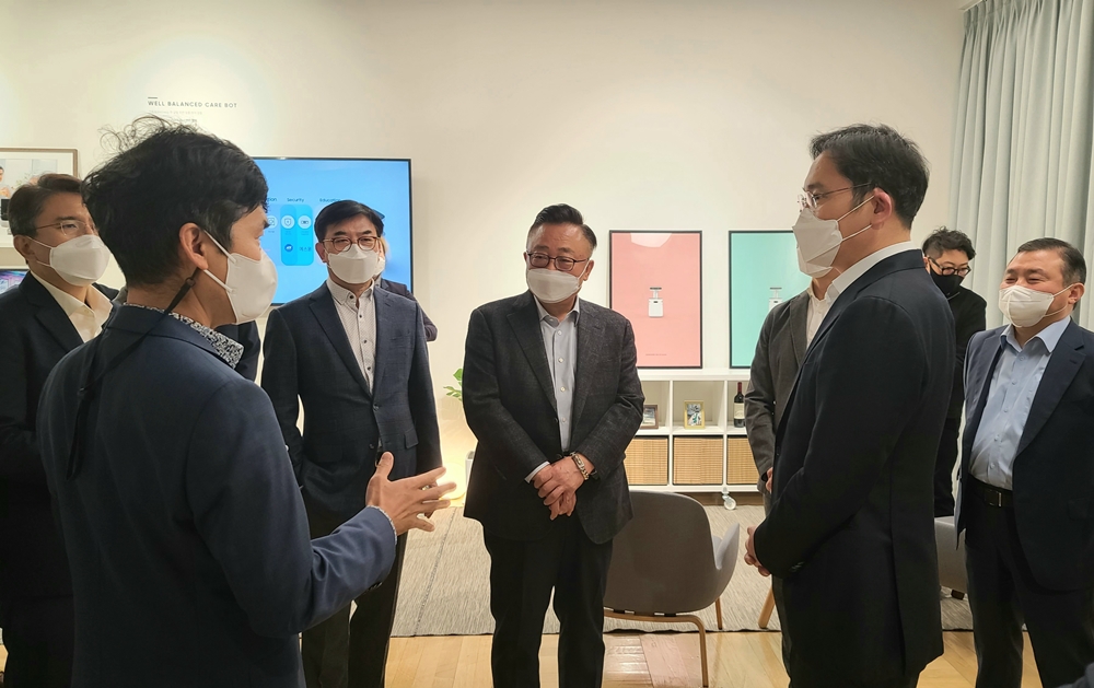
At the R&D center, Lee was briefed on Samsung's latest projects on AI, servers, and next-generation (6G) telecommunication technologies. Samsung Research is led by renowned AI expert Sebastian Seung, and he oversees the company's AI, software, and telecom technologies. He is working on improving home appliances, smartphones, and TV with human-like algorithms.
It is being said that Lee's visits to the company's plants and R&D centers will boost employee morale and encourage the company to secure its future growth engines in the post-pandemic era.
Asif is a computer engineer turned technology journalist. He has been using Samsung phones since 2004, and his current smartphone is the Galaxy S23 Ultra. He loves headphones, mechanical keyboards, and PC hardware. When not writing about technology, he likes watching crime and science fiction movies and TV shows.