Best buy guide: Galaxy Watch 6 or Galaxy S24+. Woo-hoo join SamMobile on WhatsApp or Telegram!

SamMobile has affiliate and sponsored partnerships. If you buy something through one of these links, we may earn a commission.

Notifications
    News for you

    Samsung’s 2.5D chip packing technology H-Cube is now available

    General
    By 

    Last updated: November 11th, 2021 at 07:46 UTC+01:00

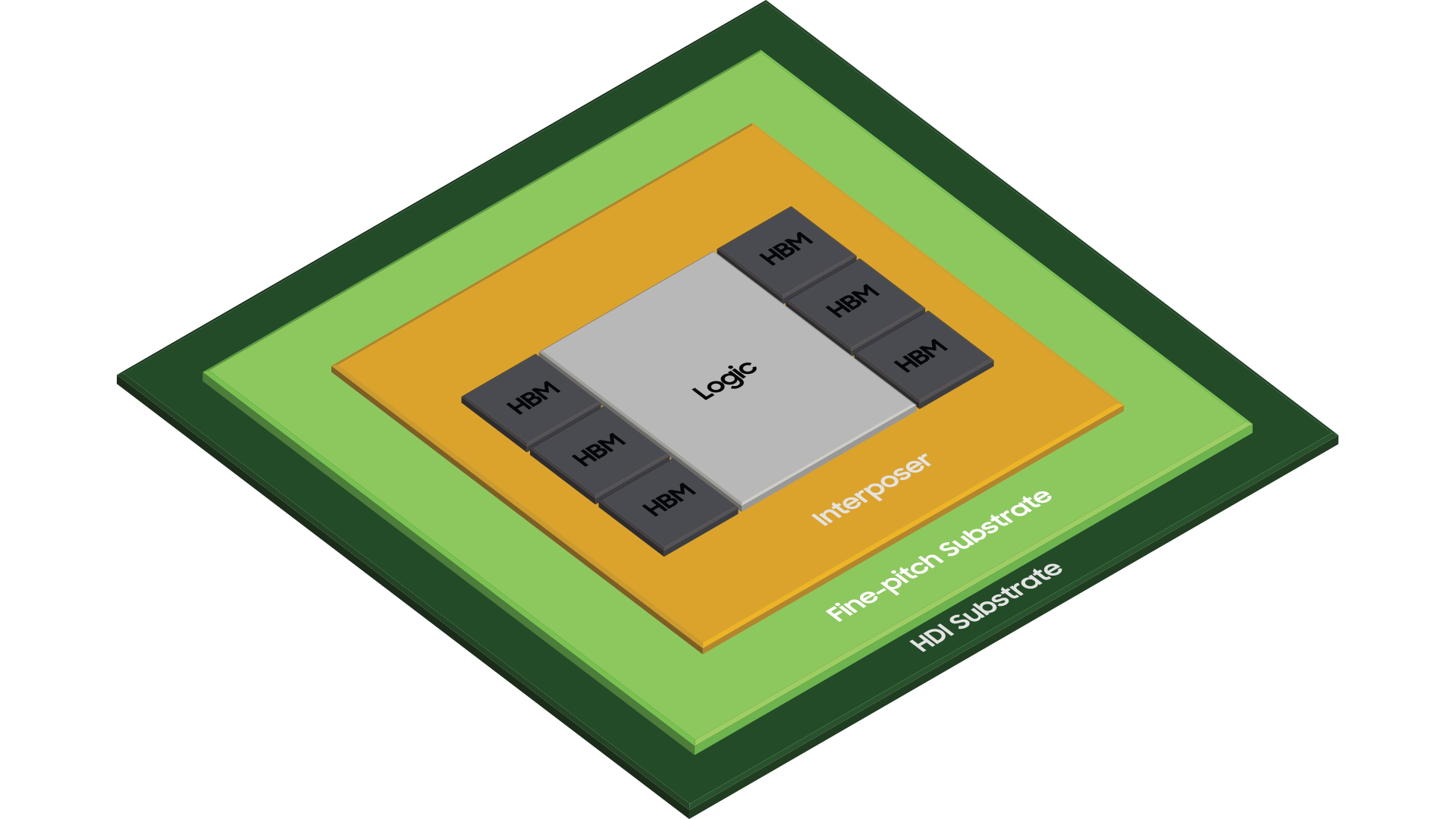
    Samsung Foundry has announced that its latest 2.5D semiconductor chip packaging technology H-Cube is now available for its foundry clients. H-Cube, which was developed in collaboration with Samsung Electro-Mechanics and Amkor Techology, allows complex logic and HBM (High-Bandwidth Memory) chips to be packed in compact sizes.

    The South Korean firm said that its new packaging technology is suitable for AI (Artificial Intelligence), data center, HPC (High-Performance Computing), and networking products that require high-performance and large-area packaging. This technology can be used to place logic chips or HBM on top of a silicon interposer in a smaller area.

    To develop this technology, Samsung Foundry used a hybrid substrate with a fine-pitch substrate and High-Density Interconnection (HDI) to fit large sizes into 2.5D packaging. With increasing computing power and storage needs, semiconductor chips can become larger in size, but 2.5D chip packaging technology like H-Cube can fit more in a smaller area and offer compact solutions.

    When fitting six or more HBMs in a single package, difficulty in making the package can increase rapidly. Samsung solved this issue by using a hybrid substrate structure that uses an easy-to-implement HDI substrate overlapped under a fine-pitch substrate. The company also used solder balls with a smaller pitch (35%) to connect the chip with the substrate.
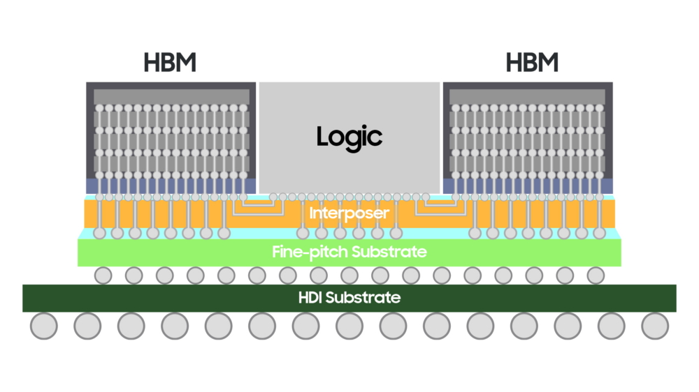
    The company also used its proprietary signal/power integrity analysis technology for a stable power supply and less distortion when stacking logic chips on top of HBM.

    said Moonsoo Kang, Senior Vice President and Head of Foundry Market Strategy Team at Samsung Electronics, said, “H-Cube solution, which is jointly developed with Samsung Electro-Mechanics (SEMCO) and Amkor Technology, is suited to high-performance semiconductors that need to integrate a large number of silicon dies. By expanding and enriching the foundry ecosystem, we will provide various package solutions to find a breakthrough in the challenges our customers are facing.

    Samsung H-Cube 2.5 Chip Packaging Technology Structure Top View

    General HBMSamsung Electro-MechanicsSamsung Foundry

    You might also like

    Samsung rival introduces cheaper 4nm chips, vows to bring 1.6nm chips in 2026

    Samsung rival introduces cheaper 4nm chips, vows to bring 1.6nm chips in 2026

    Samsung Foundry and TSMC are the world's most advanced contract chip manufacturers, and TSMC has had the upper hand over the past few years. While Samsung has been trying to up its game, it hasn't succeeded. With its 3nm chip fabrication process, the South Korean firm had hoped to win back big-name clients, but even […]

    • By Asif Iqbal Shaik
    • 3 days ago
    Apple iPhones to get 2nm chips before Galaxy phones

    Apple iPhones to get 2nm chips before Galaxy phones

    In 2022, TSMC announced that its 2nm fabrication process, dubbed N2, will be ready for mass production by 2025. Soon after that, it was reported that the chipset in Apple’s iPhone 17 Pro series phones would be the first to use TSMC’s 2nm fabrication process. However, after that, we didn’t get any update on the […]

    • By Abid Iqbal Shaik
    • 1 week ago
    Samsung is under emergency mode, switches to six-day workweek

    Samsung is under emergency mode, switches to six-day workweek

    Last year was bad for Samsung. Its revenue and profit took extreme hits, and the company has been under pressure from competition and the global economic downturn. While its profit increased in the first quarter of this year, Samsung has reportedly switched to a six-day workweek to inject a sense of crisis in its employees. […]

    • By Asif Iqbal Shaik
    • 1 week ago
    Galaxy S25’s Exynos 2500 to be more efficient than Snapdragon 8 Gen 4

    Galaxy S25’s Exynos 2500 to be more efficient than Snapdragon 8 Gen 4

    Samsung is developing the Exynos 2500 chipset, which it could offer with the Galaxy S25 series smartphones in some regions. Last year, the company confirmed that it would make the upcoming chipset on Samsung Foundry’s second-generation 3nm fabrication process, which is expected to offer better power efficiency than not only Samsung’s 4nm fabrication process that […]

    • By Abid Iqbal Shaik
    • 1 week ago
    Samsung has a grand plan to establish dominance in AI memory

    Samsung has a grand plan to establish dominance in AI memory

    The demand for high-bandwidth memory (HBM) is projected to skyrocket in the coming years as AI matures and the era of general artificial intelligence is ushered in. As one of the world's leading suppliers of memory products, Samsung understandably considers this a lucrative opportunity, and the company has put together a grand plan to establish […]

    • By Adnan Farooqui
    • 2 weeks ago
    Samsung gets $6.4 billion in incentives for its semiconductor chip plant in US

    Samsung gets $6.4 billion in incentives for its semiconductor chip plant in US

    Last month, it was reported that Samsung could get a $6 billion grant from the US government to build advanced chip factories in the US. The US government has now officially announced that it is offering $6.4 billion in grants to Samsung Electronics for its chipmaking investments in Texas. Samsung will invest $44 billion to […]

    • By Asif Iqbal Shaik
    • 2 weeks ago