Best buy guide: Galaxy Watch 6 or Galaxy S24+. Woo-hoo join SamMobile on WhatsApp or Telegram!

SamMobile has affiliate and sponsored partnerships. If you buy something through one of these links, we may earn a commission.

Notifications
    News for you

    Watch drone footage of Samsung’s semiconductor campuses in Korea

    General
    By 

    Last updated: August 28th, 2021 at 07:03 UTC+02:00

    Samsung Semiconductor is among the world's biggest semiconductor chip brands. Apart from designing and manufacturing its own chips, the company also makes chips for other brands such as Google, IBM, Nvidia, and Qualcomm. To fabricate those complicated chips, the South Korean firm has multiple state-of-the-art chip factories around the world, including in China, South Korea, and the US. Ever wondered how big they are and how they look?

    Well, the company has published a couple of videos that show its semiconductor chip campuses across South Korea through a bird's eye view. The videos were shot using drones, and they give you an idea of the massive scale at which Samsung operates.

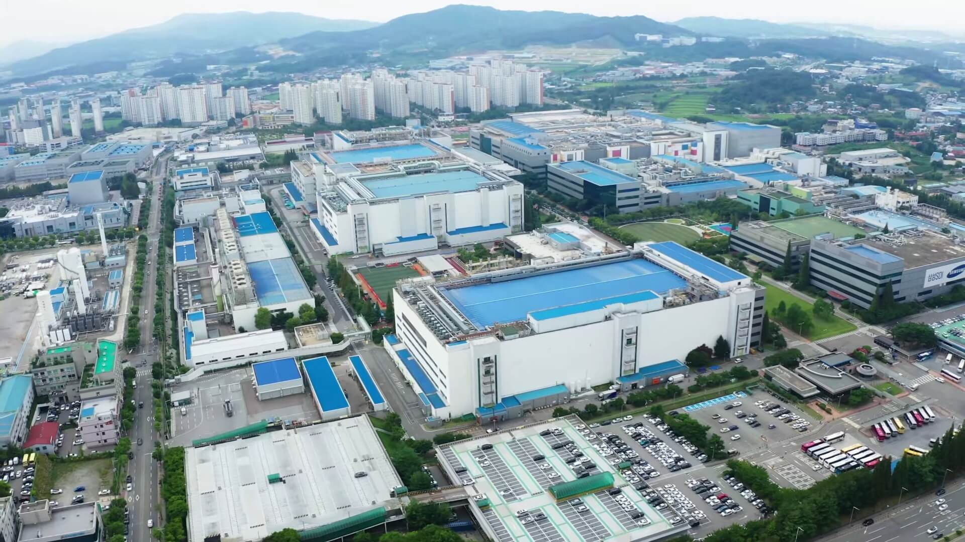
    The first video takes us through five Samsung semiconductor campuses: Hwaseong CampusGiheung Campus, Pyeongtaek Campus, Onyang Campus, and Cheonan Campus. The Hwaseong Campus is the home to Samsung's chip R&D and manufacturing facilities. There's an iconic A-shaped bridge that connects two buildings and signifies the collaboration between various teams. It also has three high-rise DSR towers that have 29 floors above the ground and four floors underground. Over 15,000 employees work here.

    The Gihueng Campus is where Samsung Electronics first started making chips. The company successfully developed 64kb DRAM in 1983, six months after its VLSI (Very Large-Scale Integration) business was established. It consists of Line 1, Samsung's first memory chip fabrication line. The Pyeongtaek Campus is the world's biggest semiconductor manufacturing complex. This is where chips are made using the cutting-edge EUV process. We can see that the company is actively expanding its campus and the construction work is ongoing.

    The Onyang Campus is situated in the hills and is responsible for the final stage of semiconductor manufacturing. It covers the development of semiconductor packaging, production, testing, and shipping of the end product. It is surrounded by lush green fields and hills. The Cheonan Campus is the future of chips where next-generation packaging technology is developed.

    The second video footage is shot using a racing drone, complete with impressive feats in the air. We can see that all campuses shown in these videos have large buildings, big parks, and wide roads.

    General Samsung ElectronicsSamsung FoundrySamsung SemiconductorSouth Korea

    You might also like

    Samsung rival introduces cheaper 4nm chips, vows to bring 1.6nm chips in 2026

    Samsung rival introduces cheaper 4nm chips, vows to bring 1.6nm chips in 2026

    Samsung Foundry and TSMC are the world's most advanced contract chip manufacturers, and TSMC has had the upper hand over the past few years. While Samsung has been trying to up its game, it hasn't succeeded. With its 3nm chip fabrication process, the South Korean firm had hoped to win back big-name clients, but even […]

    • By Asif Iqbal Shaik
    • 2 days ago
    Samsung showcases Team AI that handles your everyday chores

    Samsung showcases Team AI that handles your everyday chores

    Samsung’s 2024 lineup of Bespoke home appliances has some amazing products. However, the two that stand out are the Bespoke AI Laundry Combo and Bespoke Jet Bot Comb as they offer some of the best features in their segment. The company launched the Bespoke AI Laundry Combo in South Korea earlier this year, and the […]

    • By Abid Iqbal Shaik
    • 2 days ago
    Top-level visits underway as Samsung seeks turnaround in China

    Top-level visits underway as Samsung seeks turnaround in China

    China is an important market and while Samsung once enjoyed a considerable share in the country's smartphone market, it has since fallen to 0%. The company needs to do a lot more than just launch basic phones to revive its fortunes in the lucrative market. Samsung has set up a dedicated team to pursue a […]

    • By Adnan Farooqui
    • 2 days ago
    Samsung and Google tease new AI features

    Samsung and Google tease new AI features

    Samsung and Google have started teasing new AI (Artificial Intelligence) features developed through a partnership that's never been stronger. In a recent social media post on X, both Samsung Mobile and Google's Rick Osterloh confirmed that the two companies are continuing to work together to develop new exciting features. According to these recent teasers, Google's […]

    • By Mihai Matei
    • 3 days ago
    Samsung LATAM wants to recycle nearly 15,000 tons of e-waste in 2024

    Samsung LATAM wants to recycle nearly 15,000 tons of e-waste in 2024

    Samsung will extend its recycling and waste collection efforts to three more Latin American countries. During Earth Day earlier this week, the company announced that it will run its waste collection program in 13 countries instead of 10. Through its extended efforts, Samsung's new goal for 2024 is to collect a minimum of 14,183 tons […]

    • By Mihai Matei
    • 3 days ago
    Galaxy Z Flip smartphones may eventually get a zoom camera

    Galaxy Z Flip smartphones may eventually get a zoom camera

    One thing the Galaxy Z Flip series lacks is a telephoto camera. All the models released so far only feature wide and ultra-wide lenses, but new evidence has emerged to suggest that Samsung might eventually add a third sensor to the back of its future Galaxy Z Flip phones. A Samsung patent unearthed by GalaxyClub […]

    • By Mihai Matei
    • 3 days ago