The best Samsung deals! Galaxy Book 4 series, Watch 6, S24 Ultra or Z Flip 5! - Join SamMobile on Telegram!

SamMobile has affiliate and sponsored partnerships. If you buy something through one of these links, we may earn a commission.

Notifications
    News for you

    All Samsung semiconductor chip plants get Carbon Trust’s Triple Standard certification

    General
    By 

    Last updated: June 3rd, 2021 at 05:35 UTC+02:00

    Samsung, the world's biggest memory chip maker, has announced that all of its semiconductor chip plants have received British Carbon Trust's Triple Standard certification. It means that all those plants are designed to reduce carbon and water waste, protecting the environment as much as possible.

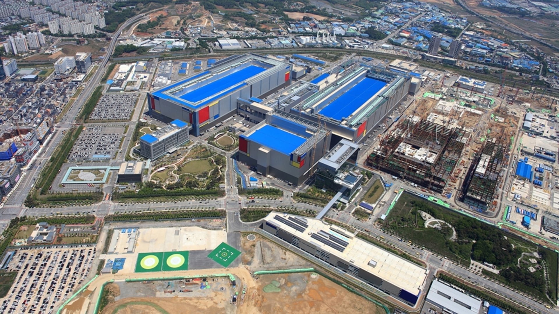
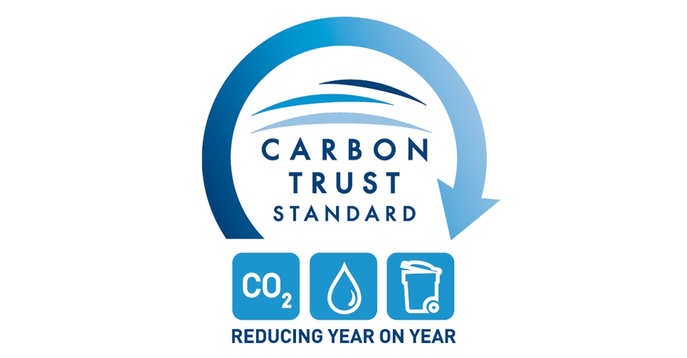
    The South Korean firm has now become the world's first company whose semiconductor manufacturing sites have received the Triple Standard certification from Carbon Trust. Samsung Foundry has a total of nine semiconductor chip plants spread across China (Suzhou, Tianjin, and Xian), South Korea (Cheonan, Giheung, Hwaseong, Onyang, Pyeongtaek), and the US (Austin, Texas).

    Samsung's chip plants have reduced carbon emissions, water wastage, and waste emissions

    As the semiconductor industry moves towards more advanced chip fabrication processes, the use of water and carbon emissions increases. However, Samsung has set up strict procedures and processes that reduce water usage as well as carbon emissions. The company has reduced carbon emissions by 9.6%, water usage by 7.8%, and waste emissions by 4.1% over the past three years.

    The company also announced that its chip plants in China and the US have completed the goal of 100% renewable energy use with a renewable energy certificate (REC). With these efforts, Samsung has been successful in reducing 1.3 million tons in carbon emissions. Its water savings reached 10.25 million tons, thanks to improved water reuse and advanced filtration methods.

    Samsung also reduced 35,752 tons of waste by increasing the usage of eco-friendly packaging materials and reducing disposable packaging (corrugated cardboard, plastic wraps, and string bundles).

    Sung-Dae Jang, Executive Vice President of Samsung Electronics’ DS Division Sustainability Management Office, said, “We have been making efforts in various fields for decades in the fields of carbon, water, and waste in order to effectively respond to climate change and have managed them as business indices. Ultra-fine process-based low-power semiconductors We will increase the sustainability of the semiconductor business by restoring the local ecosystem through eco-friendly water treatment and developing facilities to reduce greenhouse gases.

    Carbon Trust Triple Standard Samsung Semiconductor Chip Plant

    General Samsung FoundrySamsung Semiconductor

    You might also like

    Samsung unveils its HBM3E memory and new CXL memory modules

    Samsung unveils its HBM3E memory and new CXL memory modules

    Samsung is the world's biggest semiconductor memory chip maker and is often the first to launch new technologies in the segment. Today, the company unveiled its new CXL (Compute Express Link) memory modules and the HBM3E memory. These products are meant to be used in cloud servers and supercomputers for AI and other high-performance computing […]

    • By Asif Iqbal Shaik
    • 7 hours ago
    Next-gen Galaxy phones will have faster storage for on-device AI

    Next-gen Galaxy phones will have faster storage for on-device AI

    It's been a couple of years since Samsung Semiconductor announced the UFS 4.0 non-volatile memory for mobile devices. Samsung has since used UFS 4.0 for the Galaxy S23 series, the 2023 foldable phones, and the latest Galaxy S24 lineup. Now, the company is getting ready to advance to the next step. Samsung Semiconductor revealed a […]

    • By Mihai Matei
    • 7 days ago
    Samsung to launch its own AI accelerator chip called Mach-1 in 2025

    Samsung to launch its own AI accelerator chip called Mach-1 in 2025

    Samsung launched its first AI phone, the Galaxy S24, earlier this year. Before that, the South Korean firm launched its own Large Language Model (LLM) called Samsung Gauss, which powers some of the AI features on the Galaxy S24. It is reported that Samsung will launch its own AI accelerator chip next year. Samsung's first […]

    • By Asif Iqbal Shaik
    • 1 week ago
    Samsung expects $100 million revenue from chip packaging business

    Samsung expects $100 million revenue from chip packaging business

    Samsung Electronics held its 55th annual general shareholders meeting today at the Suwon Convention Center in Suwon, Gyeonggi-do, South Korea. The company revealed its strategy for this year and expects revenue of $100 from its chip packaging business. The company's 55th annual general shareholders meeting was attended by general shareholders, institutional investors, and top-level management […]

    • By Asif Iqbal Shaik
    • 1 week ago
    Samsung could get $6 billion grant from the US for chip plants

    Samsung could get $6 billion grant from the US for chip plants

    Samsung Electronics, one of the biggest chip-making firms worldwide, has grand plans to make advanced semiconductor chips in the US. To help with its plans, the US government had announced grants and tax sops. The South Korean firm is now close to getting a huge helping hand from the US government. A $6 billion grant […]

    • By Asif Iqbal Shaik
    • 2 weeks ago
    Samsung may use SK Hynix’s method to manufacture HBM3 chips

    Samsung may use SK Hynix’s method to manufacture HBM3 chips

    According to a new report from Reuters, Samsung Electronics will soon start using the same technology as SK Hynix does to manufacture HBM3 chips. Samsung uses the non-conductive film (NCF) method to stack layers of chips in high bandwidth memory (HBM) chips. Reportedly, this method works well for chips with a lower number of layers […]

    • By Abid Iqbal Shaik
    • 2 weeks ago