Last updated: July 10th, 2018 at 09:50 UTC+02:00
SamMobile has affiliate and sponsored partnerships, we may earn a commission.
Reading time: 2 minutes
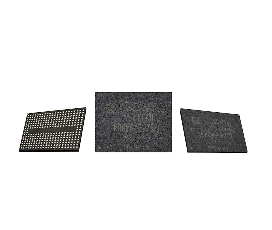
The industry's first use of Toggle DDR 4.0 interface enables the data transfer speed between storage and memory over Samsung's new 256Gb V-NAND has crossed 1.4Gbps which is a 40 percent improvement over its 64-layer predecessor.
There are more than 90 layers of “3D charge trap flash (CTF) cells” inside Samsung's fifth-generation V-NAND which is the largest amount in the industry. They're stacked in a pyramid structure with microscopic channel holes vertically drilled throughout. The channel holes are only a few hundred nanometers wide and contain over 85 billion CTF cells that can store three bits of data each.
Despite the bump in performance, Samsung says that the energy efficiency of the new chip is comparable to that of the 64-layer chip. That's largely because the operating voltage has been reduced from 1.8 volts to 1.2 volts. The new V-NAND chip also offers the fastest data write speed of 500-microseconds. It's an improvement of 30 percent over the write speed of the predecessor. The response time to read signals has been reduced significantly to 50μs.
Samsung also announced today that it's preparing to introduce 1Tb and quad-level cell offerings to its V-NAND lineup eventually. Samsung's new high-performance memory chip will be used in a variety of devices including but not limited to premium smartphones.

Adnan Farooqui is a long-term writer at SamMobile. Based in Pakistan, his interests include technology, finance, Swiss watches and Formula 1. His tendency to write long posts betrays his inclination to being a man of few words.